DARPA-funded researchers have developed one of the world’s largest and most complex computer chips ever produced—one whose architecture is inspired by the neuronal structure of the brain and requires only a fraction of the electrical power of conventional chips.
Designed by researchers at IBM in San Jose, California, under DARPA’s Systems of Neuromorphic Adaptive Plastic Scalable Electronics (SyNAPSE) program, the chip is loaded with more than 5 billion transistors and boasts more than 250 million “synapses,” or programmable logic points, analogous to the connections between neurons in the brain. That’s still orders of magnitude fewer than the number of actual synapses in the brain, but a giant step toward making ultra-high performance, low-power neuro-inspired systems a reality.
Many tasks that people and animals perform effortlessly, such as perception and pattern recognition, audio processing and motor control, are difficult for traditional computing architectures to do without consuming a lot of power. Biological systems consume much less energy than current computers attempting the same tasks. The SyNAPSE program was created to speed the development of a brain-inspired chip that could perform difficult perception and control tasks while at the same time achieving significant energy savings.
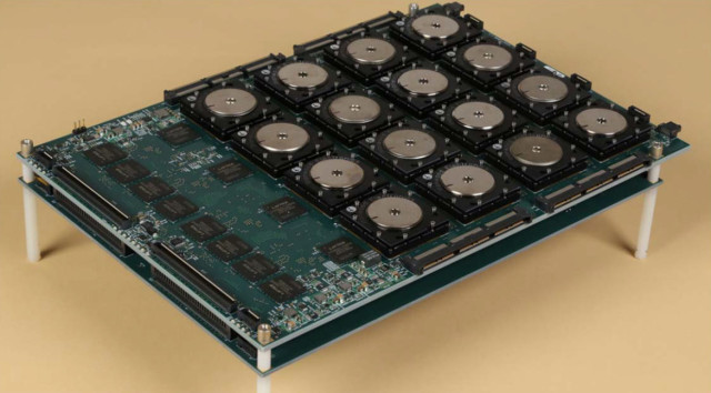
The SyNAPSE-developed chip, which can be tiled to create large arrays, has one million electronic “neurons” and 256 million electronic synapses between neurons. Built on Samsung Foundry’s 28nm process technology, the 5.4 billion transistor chip has one of the highest transistor counts of any chip ever produced. Each chip consumes less than 100 milliWatts of electrical power during operation. When applied to benchmark tasks of pattern recognition, the new chip achieved two orders of magnitude in energy savings compared to state-of-the-art traditional computing systems.
The high energy efficiency is achieved, in part, by distributing data and computation across the chip, alleviating the need to move data over large distances. In addition, the chip runs in an asynchronous manner, processing and transmitting data only as required, similar to how the brain works. The new chip’s high energy efficiency makes it a candidate for defense applications such as mobile robots and remote sensors where electrical power is limited.
“Computer chip design is driven by a desire to achieve the highest performance at the lowest cost. Historically, the most important cost was that of the computer chip. But Moore’s law—the exponentially decreasing cost of constructing high-transistor-count chips—now allows computer architects to borrow an idea from nature, where energy is a more important cost than complexity, and focus on designs that gain power efficiency by sparsely employing a very large number of components to minimize the movement of data. IBM’s chip, which is by far the largest one yet made that exploits these ideas, could give unmanned aircraft or robotic ground systems with limited power budgets a more refined perception of the environment, distinguishing threats more accurately and reducing the burden on system operators,” said Gill Pratt, DARPA program manager. “Our troops often are in austere environments and must carry heavy batteries to power mobile devices, sensors, radios and other electronic equipment. Air vehicles also have very limited power budgets because of the impact of weight. For both of these environments, the extreme energy efficiency achieved by the SyNAPSE program’s accomplishments could enable a much wider range of portable computing applications for defense.”
Another potential application for the SyNAPSE-developed chip is neuroscience modelling. The large number of electronic neurons and synapses in each chip and the ability to tile multiple chips could lead to the development of complex, networked neuromorphic simulators for testing network models in neurobiology and deepening current understanding of brain function.
A technical paper on the new chip is available here.
Photo:A circuit board shows 16 of the new brain-inspired chips in a 4 X 4 array along with interface hardware. The board is being used to rapidly analyze high-resolutions images. Courtesy: IBM
Source: DARPA

